Semiconductor Electronics | Physics - Short Answer Questions | 12th Physics : UNIT 10a : Semiconductor Electronics
Chapter: 12th Physics : UNIT 10a : Semiconductor Electronics
Short Answer Questions
Short Answer Questions
1. Define forbidden
energy gap.
The
energy gap between the valence band and the conduction band is called forbidden
energy gap.
2. Why is
temperature co-efficient of resistance negative for semiconductor?
At
a finite temperature, a semiconductor has very small electrical conductivity.
When the temperature is increased further, more number of electrons are
promoted to the conduction band and they increase the conduction.
Thus,
the electrical conduction increases with the increase in temperature. In other
words, resistance decreases with increase in temperature.
Hence,
semiconductors have negative temperature coefficient of resistance.
3. What do you mean
by doping?
The
process of adding impurities to the intrinsic semiconductor is called doping.
It
increases the concentration of charge carriers in the semiconductor. So, its
electrical conductivity is increases.
The impurity atoms are called dopants.
4. Distinguish
between intrinsic and extrinsic semiconductors.
Intrinsic semiconductor
•
A semiconductor in its pure form without impurity is called an intrinsic
semiconductor
•
The number of free electrons is equal to the number of holes.
•
In it, electrical conductivity is the function of temperature alone
•
Fermi energy level lies at the centre of forbidden energy gap.
Extrinsic semiconductor
•
When a small amount of impurity is doped in pure semiconductor it becomes extrinsic
semiconductor
•
The number of free electrons and hole never equal. In n-type majority carriers
are electrons. In p-type majority carriers are holes.
•
In it, electrical conductivity is the function of temperature as well as concentration
of impurity atoms doped in it.
•
In n-type Fermi level is just below the conduction band where as in p-type
Fermi energy level is just above the valance band.
5. A diode is
called as a unidirectional device.
Explain.
i)
A dipole is unidirectional, ie. current flows in only one direction.
ii)
When a forward bias is applied, the diode conducts, and when a reverse bias is
applied, there is no conduction.
iii)
Diode will conduct when the potential difference between the anode and the
cathode exceeds the barrier voltage. 0.3V for Ge and 0.7V for Si.
6. What do you mean
by leakage current in a diode?
Under
reverse bias, a very small current in ÎĽA flows across the junction in a diode.
This is due to the flow of minority charge carriers called leakage current (or)
reverse saturation current.
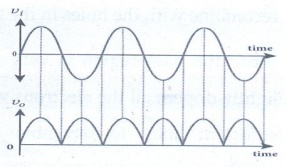
7. Draw the output
waveform of a full wave rectifier.
8. Distinguish between avalanche and Zener breakdown
Avalanche Breakdown
•
When both sides of the PN junction are lightly doped and the depletion layer
becomes large.
•
The electric field across the depletion layer is not so strong.
•
Due to the collision, covalent bonds are broken and electron hole pairs are
generated.
•
Reverse voltage must be greater than 6V
Zener breakdown
•
When both sides of the PN junction heavily doped and the depletion Layer is
narrow
•
A very strong electric field is produced across the thin depletion layer.
•
Due to strong electric field, the covalent bonds breaks and large number of electrons
and holes are produced.
•
Reverse voltage must be less than 4V
9. Give the
Barkhausen conditions for sustained oscillations.
*
The loop phase shift must be 0° or integral multiple of 2π
*
The loop gain must be unity |Aβ| = 1
10. Explain the
current flow in a NPN transistor.
i)
In an NPN transistor, the majority carriers in the emitter are electrons.
ii)
As it is heavily doped, it has a large number of electrons.
iii)
The forward bias across the emitter base junction causes the electrons in the
emitter region to flow towards the base region and constitutes the emitter
current (IE).
iv)
The electrons after reaching the base region recombine with the holes in the
base region.
v)
Since the base region is very narrow and lightly doped, all the electrons will
not have sufficient holes to recombine and hence most of the electrons reach
the collector region.
11. What are logic
gates?
A
logic gate is an electronic circuit whose function is based on digital signals
They are binary in nature.
The
logic gates are the basic building blocks of most of the digital systems.
They
have one output with one or more inputs.
12. Explain the
need for a feedback circuit in a transistor oscillator.
The
circuit used to feedback, a portion of the output to the input is called the
feedback network. If the portion of the output fed to the input is in phase
with the input, then the magnitude of the input signal increases. It is
necessary for sustained oscillations.
13. Write a short
note on diffusion current across p-n junction.
Whenever
p-n junction is formed, some of the free electrons diffuse from the n-side to
the p-side while the holes from the p-side to the n side.
The
diffusion of charge carriers happens due to the n-side has higher electron
concentration and the p-side has higher hole concentration.
The
diffusion of the majority charge carriers across the junction gives rise to an
electric current, called diffusion current.
14. What is meant
by biasing? Mention its types.
Biasing
means providing external energy to charge carriers to overcome the barrier
potential and make them move in a particular direction.
We
have two types of biasing:
(i)
Forward bias
(ii)
Reverse bias
15. Why can't we
interchange the emitter and collector even though they are made up of the same
type of semiconductor material?
The
emitter is more heavily doped than the collector and it is made physically
smaller than the collector.
The
collector is physically larger than the other two regions.
Because
of the differing size and the amount of doping, the emitter and collector
cannot be interchanged.
16. Why are NOR and
NAND gates called universal gates?
NAND
and NOR gates are known as universal gates because all other basic logic gates
can be made from NAND or NOR gates.
17. Define barrier
potential.
The
difference in potential across the depletion layer is called the barrier
potential.
At
25°C, this barrier potential is approximately 0.7V for silicon and 0.3V for
germanium.
18. What is
rectification?
The
process in which alternating voltage or alternating current is converted into
direct voltage or direct current is known as rectification.
The
device used for this process is called as rectifier.
19. List the
applications of Light Emitting Diode LED?
a)
Indicator lamp
b)
Seven segment display
c)
Traffic signals, exit signs, emergency vehicle lighting etc...
d)
Industrial process control, position encoders, bar graph readers.
20. Give the
principle of solar cells.
A
solar cell, also known as photovoltaic cell, works on the principle of
photovoltaic effect.
Accordingly,
the p-n junction of the solar cell generates emf when solar radiation falls on
it.
21. What is an
integrated circuit?
An
integrated circuit consists of thousands to millions of transistors, resistors,
capacitors integrated on a small flat piece of semiconductor material that is
normally silicon.
It
is also called as an IC or a chip or a microchip.
22. What is
modulation?
For
long distance transmission, the low frequency baseband signal is superimposed
onto a high frequency radio signal by a process called modulation.
23. Define
bandwidth of transmission system.
The
range of frequencies required to transmit a piece of specified information in a
particular channel is called channel bandwidth or the bandwidth of the
transmission system.
24. What is meant
by skip distance and skip zone?
Skip Distance:
In
the sky wave propagation the shortest distance between the point of
transmission and the point of reception along the surface is known as the skip
distance
Skip Zone / Skip area:
In
sky wave propagation, there is a zone where there is no reception of
electromagnetic waves neither ground nor sky, called as skip zone (or) skip
area.
25. Give
applications of RADAR.
i)
In military, it is used for locating and detecting the targets.
ii)
It is used in navigation systems such as ship borne surface search, air search
and missile guidance systems.
iii)
Radars are used to measure precipitation rate and wind speed in meteorological
observations.
iv)
It is employed to locate and rescue people in emergency situations.
26. What is mobile
communication?
Mobile
communication is used to communicate with others in different locations without
the use of any physical connection like wires or cables.
27. Explain centre
frequency or resting frequency in frequency modulation.
When
the frequency of the baseband signal is zero, there is no change in the
frequency of the carrier wave. It is at its normal frequency and is called as
centre frequency or resting frequency.
28. What does RADAR
stand for?
RADAR
basically stands for Radio Detection And Ranging System
Related Topics